- 您现在的位置:买卖IC网 > Sheet目录2005 > LTC2251IUH#PBF (Linear Technology)IC ADC 10-BIT 125MSPS 3V 32-QFN
LTC2251/LTC2250
15
22510fa
APPLICATIO S I FOR ATIO
WU
UU
sample-and-hold charging glitches and limiting the
wideband noise at the converter input.
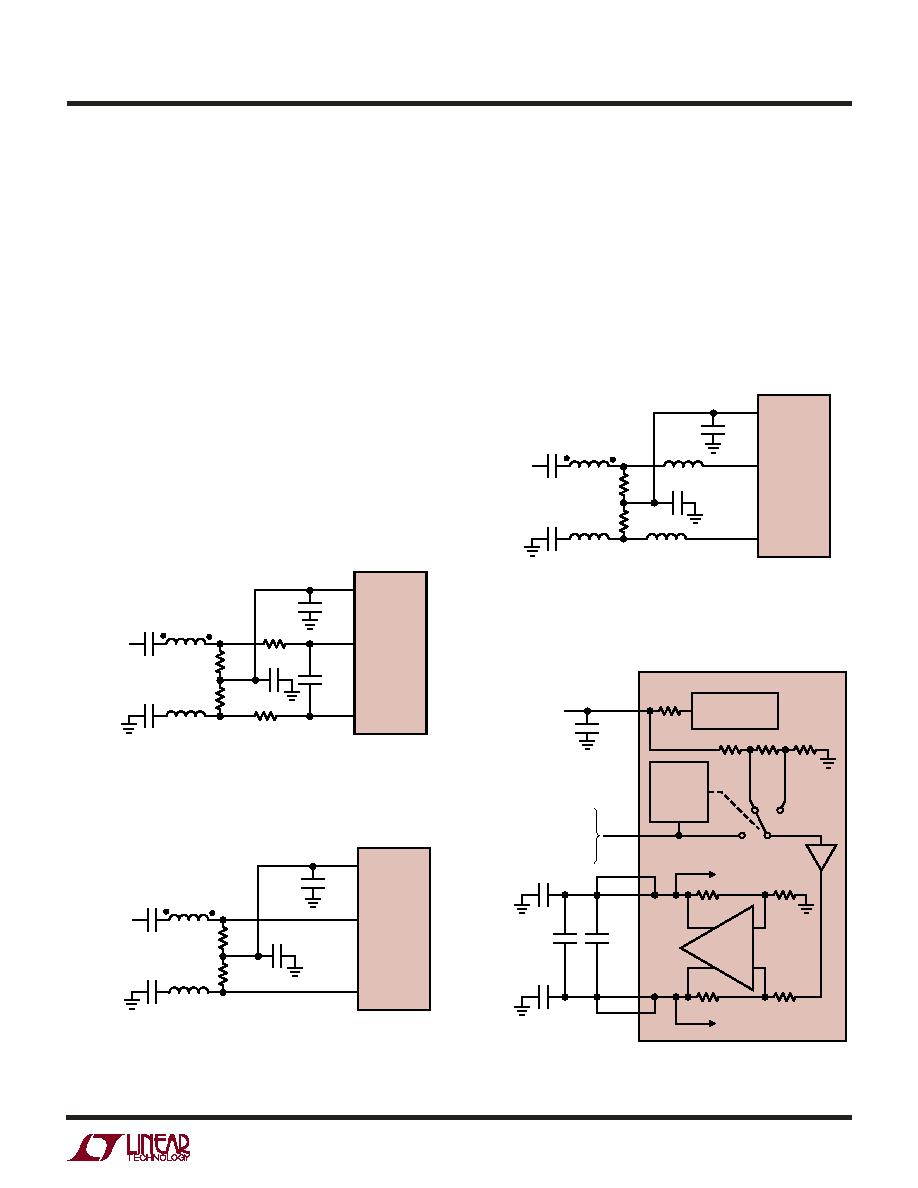
For input frequencies above 70MHz, the input circuits of
Figure 6, 7 and 8 are recommended. The balun transformer
gives better high frequency response than a flux coupled
center tapped transformer. The coupling capacitors allow
the analog inputs to be DC biased at 1.5V. In Figure 8, the
series inductors are impedance matching elements that
maximize the ADC bandwidth.
Reference Operation
Figure 9 shows the LTC2251/LTC2250 reference circuitry
consisting of a 1.5V bandgap reference, a difference am-
plifier and switching and control circuit. The internal volt-
age reference can be configured for two pin selectable input
ranges of 2V (
±1V differential) or 1V (±0.5V differential).
Tying the SENSE pin to VDD selects the 2V range; tying the
SENSE pin to VCM selects the 1V range.
Figure 6. Recommended Front End Circuit for
Input Frequencies Between 70MHz and 170MHz
25
25
12
12
0.1
F
AIN
+
AIN
–
8pF
2.2
F
VCM
ANALOG
INPUT
0.1
F
0.1
F
T1
T1 = MA/COM, ETC 1-1-13
RESISTORS, CAPACITORS
ARE 0402 PACKAGE SIZE
22510 F06
LTC2251/
LTC2250
Figure 8. Recommended Front End Circuit for
Input Frequencies Above 300MHz
25
25
0.1
F
AIN
+
AIN
–
2.2
F
VCM
ANALOG
INPUT
0.1
F
0.1
F
T1
T1 = MA/COM, ETC 1-1-13
RESISTORS, CAPACITORS, INDUCTORS
ARE 0402 PACKAGE SIZE
22510 F08
8.2nH
LTC2251/
LTC2250
Figure 7. Recommended Front End Circuit for
Input Frequencies Between 170MHz and 300MHz
25
25
0.1
F
AIN
+
AIN
–
2.2
F
VCM
ANALOG
INPUT
0.1
F
0.1
F
T1
T1 = MA/COM, ETC 1-1-13
RESISTORS, CAPACITORS
ARE 0402 PACKAGE SIZE
22510 F07
LTC2251/
LTC2250
The 1.5V bandgap reference serves two functions: its
output provides a DC bias point for setting the common
mode voltage of any external input circuitry; additionally,
the reference is used with a difference amplifier to gener-
ate the differential reference levels needed by the internal
ADC circuitry. An external bypass capacitor is required for
the 1.5V reference output, VCM. This provides a high
frequency low impedance path to ground for internal and
external circuitry.
VCM
REFH
SENSE
TIE TO VDD FOR 2V RANGE;
TIE TO VCM FOR 1V RANGE;
RANGE = 2 VSENSE FOR
0.5V < VSENSE < 1V
1.5V
REFL
2.2
F
2.2
F
INTERNAL ADC
HIGH REFERENCE
BUFFER
0.1
F
22510 F09
4
DIFF AMP
1
F
1
F
INTERNAL ADC
LOW REFERENCE
1.5V BANDGAP
REFERENCE
1V
0.5V
RANGE
DETECT
AND
CONTROL
LTC2251/LTC2250
Figure 9. Equivalent Reference Circuit
发布紧急采购,3分钟左右您将得到回复。
相关PDF资料
LTC2253IUH#TRPBF
IC ADC 12BIT 125MSPS 3V 32-QFN
LTC2255CUH#TRPBF
IC ADC 14BIT 125MSPS 3V 32-QFN
LTC2258IUJ-12#PBF
IC ADC 12BIT 65MSPS 1.8V 40-QFN
LTC2262CUJ-14#TRPBF
IC ADC 14BIT 150MSPS 40-QFN
LTC2262IUJ-12#PBF
IC ADC 12BIT 150MSPS 40-QFN
LTC2264CUJ-12#PBF
IC ADC 12BIT SER/PAR 40M 40-QFN
LTC2268IUJ-14#TRPBF
IC ADC 14BIT 125MSPS DUAL 40QFN
LTC2280CUP#PBF
IC ADC DUAL 10BIT 105MSPS 64-QFN
相关代理商/技术参数
LTC2251IUH#TRPBF
功能描述:IC ADC 10BIT 125MSPS 3V 32-QFN RoHS:是 类别:集成电路 (IC) >> 数据采集 - 模数转换器 系列:- 标准包装:1,000 系列:- 位数:12 采样率(每秒):300k 数据接口:并联 转换器数目:1 功率耗散(最大):75mW 电压电源:单电源 工作温度:0°C ~ 70°C 安装类型:表面贴装 封装/外壳:24-SOIC(0.295",7.50mm 宽) 供应商设备封装:24-SOIC 包装:带卷 (TR) 输入数目和类型:1 个单端,单极;1 个单端,双极
LTC2252
制造商:LINER 制造商全称:Linear Technology 功能描述:14-Bit, 125/105Msps Low Power 3V ADCs
LTC2252CUH
制造商:Linear Technology 功能描述:Single ADC Pipelined 105Msps 12-bit Parallel 32-Pin QFN EP
LTC2252CUH#PBF
功能描述:IC ADC 12-BIT 105MSPS 3V 32-QFN RoHS:是 类别:集成电路 (IC) >> 数据采集 - 模数转换器 系列:- 标准包装:1 系列:microPOWER™ 位数:8 采样率(每秒):1M 数据接口:串行,SPI? 转换器数目:1 功率耗散(最大):- 电压电源:模拟和数字 工作温度:-40°C ~ 125°C 安装类型:表面贴装 封装/外壳:24-VFQFN 裸露焊盘 供应商设备封装:24-VQFN 裸露焊盘(4x4) 包装:Digi-Reel® 输入数目和类型:8 个单端,单极 产品目录页面:892 (CN2011-ZH PDF) 其它名称:296-25851-6
LTC2252CUH#TRPBF
功能描述:IC ADC 12BIT 105MSPS 3V 32-QFN RoHS:是 类别:集成电路 (IC) >> 数据采集 - 模数转换器 系列:- 标准包装:1 系列:- 位数:14 采样率(每秒):83k 数据接口:串行,并联 转换器数目:1 功率耗散(最大):95mW 电压电源:双 ± 工作温度:0°C ~ 70°C 安装类型:通孔 封装/外壳:28-DIP(0.600",15.24mm) 供应商设备封装:28-PDIP 包装:管件 输入数目和类型:1 个单端,双极
LTC2252IUH
制造商:Linear Technology 功能描述:ADC Single Pipelined 105Msps 12-bit Parallel 32-Pin QFN EP
LTC2252IUH#PBF
功能描述:IC ADC 12-BIT 105MSPS 3V 32-QFN RoHS:是 类别:集成电路 (IC) >> 数据采集 - 模数转换器 系列:- 标准包装:1 系列:microPOWER™ 位数:8 采样率(每秒):1M 数据接口:串行,SPI? 转换器数目:1 功率耗散(最大):- 电压电源:模拟和数字 工作温度:-40°C ~ 125°C 安装类型:表面贴装 封装/外壳:24-VFQFN 裸露焊盘 供应商设备封装:24-VQFN 裸露焊盘(4x4) 包装:Digi-Reel® 输入数目和类型:8 个单端,单极 产品目录页面:892 (CN2011-ZH PDF) 其它名称:296-25851-6
LTC2252IUH#PBF
制造商:Linear Technology 功能描述:A/D Converter (A-D) IC 制造商:Linear Technology 功能描述:IC, ADC, 12BIT, 105MSPS, QFN-32